Revolutionizing EUV Lithography with Imec’s Post-Exposure Bake Innovation
Chipmakers face relentless pressure to improve EUV lithography efficiency as semiconductor nodes shrink. Imec’s recent breakthrough in post-exposure bake (PEB) technology offers a promising solution, delivering a 20% improvement in photoresist performance through optimized oxygen concentration. This advancement directly impacts EUV scanner throughput and cost efficiency, marking a significant step forward in advanced chip manufacturing.
Understanding the EUV PEB Challenge
Post-exposure bake is a critical step in EUV lithography where wafers are heated after exposure to solidify patterns. Traditional PEB processes use ambient air (21% oxygen), but Imec’s research reveals that increasing oxygen levels to 50% during this phase dramatically enhances metal-oxide resist (MOR) performance. This improvement allows for lower EUV doses, reducing exposure time and costs.
Key Benefits of Enhanced Oxygen Concentration
- 20% faster photo-speed in MOR materials
- 15-20% reduction in EUV dose requirements
- Improved line-edge roughness for critical layers
- Enhanced throughput for High-NA EUV systems
The BEFORCE Tool: Enabling Controlled PEB Environments
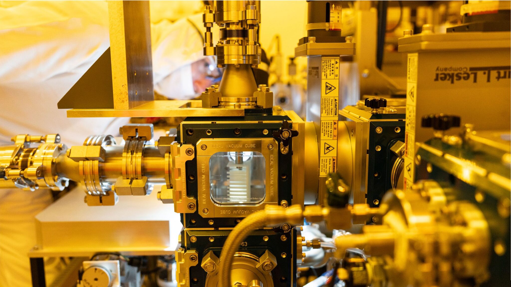
Imec developed the BEFORCE (Bake and EUV system with FTIR and Outgas measurement for Resist evaluation in Controlled Environment) tool to test these innovations. This specialized equipment allows precise control of gas composition during PEB, isolating wafers from standard cleanroom conditions. The system’s gas injection capabilities enable researchers to study environmental effects on lithographic variability while maintaining material stability.
Technical Advantages of BEFORCE
- Regulates oxygen levels from 21% to 50%
- Integrates photo-speed metrology for real-time performance tracking
- Minimizes contamination risks during wafer handling
- Supports both experimental and commercial MOR materials
Implications for the Semiconductor Industry
This innovation addresses two major challenges in EUV manufacturing: throughput limitations and cost efficiency. By reducing EUV exposure times, foundries can produce more wafers per hour without requiring new equipment investments. However, industrializing this method requires collaboration with tool manufacturers to adapt existing PEB modules with controlled gas environments.
Challenges to Adoption
- Tool redesign costs for gas injection systems
- Material stability concerns with higher oxygen exposure
- Process control complexities for CD and LER consistency
- Safety protocols for enriched oxygen environments
Future Outlook and Industry Impact
Imec’s research opens new avenues for EUV optimization, particularly as High-NA systems become mainstream. While the immediate cost savings may not directly affect consumer prices, the cumulative effect on production capacity will be significant. Equipment manufacturers like ASML will need to integrate these findings into next-generation PEB tools to maintain competitive throughput rates.
As semiconductor nodes approach 1.4nm and beyond, innovations like Imec’s oxygen-enhanced PEB will become essential. The ability to fine-tune environmental conditions during critical manufacturing steps represents a paradigm shift in EUV lithography optimization.